Semiconductor diode
A semiconductor diode is a two-terminal device that conducts current in only one direction, made of two or more layers of which at least one is a semiconductor. An example is the pn-diode, made by joining a p-type semiconducting layer to an n-type semiconducting layer.
The figure shows two structures used for pn-semiconductor diodes, both adapted to increase the voltage the devices can withstand in reverse bias. The top structure uses a mesa to avoid a sharp curvature of the p+-region next to the adjoining n-layer. The bottom structure uses a lightly doped p-guard-ring at the edge of the sharp corner of the p+-layer to spread the voltage out over a larger distance and reduce the electric field.
Electrical behavior
The ideal diode has zero resistance for the forward bias polarity, and infinite resistance (conducts zero current) for the reverse voltage polarity. In other words, the semiconductor diode acts as an electrical rectifier.
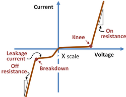
The semiconductor diode is not ideal. As shown in the figure, the diode does not conduct appreciably until a nonzero knee voltage (also called the turn-on voltage or the cut-in voltage) is reached. Above this voltage the slope of the current-voltage curve is not infinite (on-resistance is not zero). In the reverse direction the diode conducts a nonzero leakage current (exaggerated by a smaller scale in the figure) and at a sufficiently large reverse voltage below the breakdown voltage the current increases very rapidly with more negative reverse voltages.
As shown in the figure, the on and off resistances are the reciprocal slopes of the current-voltage characteristic at a selected bias point:
where rD is the resistance and ΔiD is the current change corresponding to the diode voltage change ΔvD at the bias vD=VBIAS.
Types
Semiconductor diodes come in a large variety of types:
- pn-diode: The pn junction diode consists of an n-type semiconductor joined to a p-type semiconductor.
- Zener diode: The Zener diode is a special type of pn-diode made to operate in the reverse breakdown region, and used often as a voltage regulator. The breakdown voltage in these diodes is sometimes called the Zener voltage. Depending upon the voltage range designed for, the diode may break down by either Zener breakdown, an electron tunneling behavior, or by avalanche breakdown.
- Schottky diode: The Schottky diode is made using a metal such as aluminum or platinum, on a lightly doped semiconductor substrate.
- Tunnel diode: Like the Zener diode, the tunnel diode (or Esaki diode) is made up of heavily doped n- and p-type layers with a very abrupt transition between the two types. Conduction takes place by electron tunneling.
- Light-emitting diode: The light-emitting diode is designed to convert electrical current into light.
- Photodiode: The photodiode is the inverse of the light-emitting diode, acting as a photodetector, converting incident light to a detectable electric current.
- pin-diode: The pin-diode is made of three layers: an intrinsic (undoped) layer between the p- and n-type layers. Because of its rapid switching characteristics it is used in microwave and radio-frequency applications.
- Gunn diode: The Gunn diode is a transferred electron device based upon the Gunn effect in III-V semiconductors, and is used to generate microwave oscillations.
- Varactor: a pn-junction used in reverse bias as a voltage-variable capacitor for tuning radio receivers. The term varactor also is used for devices that behave like back-to-back Zener diodes.
Operation
Here, the operation of the simple pn junction diode is considered. The objective is to explain the various bias regimes in the figure. Operation is described using band-bending diagrams that show how the lowest conduction band energy and the highest valence band energy vary with position inside the diode under various bias conditions. For additional discussion, see the article Semiconductor.
Zero bias
The figure shows a band bending diagram for a pn-diode; that is, the band edges for the conduction band (upper line) and the valence band (lower line) are shown as a function of position on both sides of the junction between the p-type material (left side) and the n-type material (right side). When a p-type and an n-type region of the same semiconductor are brought together and the two diode contacts are short-circuited, the Fermi half-occupancy level (dashed horizontal straight line) is situated at a constant level. This level insures that in the field-free bulk on both sides of the junction the hole and electron occupancies are correct. (So, for example, it is not necessary for an electron to leave the n-side and travel to the p-side through the short circuit to adjust the occupancies.)
However, a flat Fermi level requires the bands on the p-type side to move higher than the corresponding bands on the n-type side, forming a step or barrier in the band edges, labeled φB. This step changes the electron density on the n-side to become a Boltzmann factor exp(−φB/Vth) smaller on the p-side, to correspond to the lower electron density in p-region. Here the symbol Vth denotes the thermal voltage, Vth=kBT/q ≈ 25 mV at T=290 kelvins. Similar considerations apply for the effect of the barrier upon the hole density in the n-region. It so happens that the pn-product of the carrier densities is:
at any position within the diode at equilibrium.[1] Here pB, nB are the bulk majority carrier densities on the p-side and the n-side.
As a result of this step in band edges, a depletion region near the junction becomes depleted of both holes and electrons, forming an insulating region with almost no mobile charges. There are, however, fixed, immobile charges due to dopant ions. The near absence of mobile charge in the depletion layer means that the mobile charges present are insufficient to balance the immobile charge contributed by the dopant ions: a negative charge on the p-type side due to acceptor dopant and as a positive charge on the n-type side due to donor dopant. Because of this charge there is an electric field in this region, as determined by Poisson's equation. The width of the depletion region adjusts so the negative acceptor charge on the p-side exactly balances the positive donor charge on the n-side, so there is no electric field outside the depletion region on either side.
In this band configuration no voltage is applied and no current flows through the diode. To force current through the diode a forward bias must be applied, as described next.
Forward bias
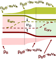
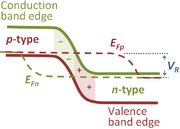
Quasi-Fermi levels and carrier densities in forward biased pn-diode. The figure assumes recombination is confined to the regions where majority carrier concentration is near the bulk values, which is not accurate when recombination-generation centers in the field region play a role.
In forward bias, electrons are injected into the p-material and holes into the n-material. The electrons in the n-type material are called majority carriers on that side, but any that make it to the p-type side are called minority carriers. The same descriptors apply to holes: they are majority carriers on the p-type side, and minority carriers on the n-type side.
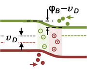
A forward bias separates the two bulk half-occupancy levels by the amount of the applied voltage, which lowers the separation of the p-type bulk band edges to be closer in energy to those of the n-type. As shown in the diagram, the step in band edges is reduced by the applied voltage to φB−vD. (The band bending diagram is made in units of volts, so no electron charge appears to convert vD to energy.)
Under forward bias, a diffusion current flows (that is a current driven by a concentration gradient) of holes from the p-side into the n-side, and of electrons in the opposite direction from the n-side to the p-side. The gradient driving this transfer is set up as follows: in the bulk distant from the interface, minority carriers have a very low concentration compared to majority carriers, for example, electron density on the p-side (where they are minority carriers) is a factor exp(−φB/Vth) lower than on the n-side (where they are majority carriers). On the other hand, near the interface, application of voltage vD reduces the step in band edges and increases minority carrier densities by a Boltzmann factor exp(vD/Vth) above the bulk values. Within the junction, the pn-product is increased above the equilibrium value to:[1]
The gradient driving the diffusion is then the difference between the large excess minority carrier densities near the interface and the low densities in the bulk, and that gradient drives diffusion of minority carriers from the interface into the bulk. The injected minority carriers are reduced in number as they travel into the bulk by recombination mechanisms that drive the excess concentrations toward the bulk values.
Recombination can occur by direct encounter with a majority carrier, annihilating both carriers, or through a recombination-generation center, a defect that alternately traps holes and electrons, assisting recombination. The minority carriers have a limited lifetime, and this lifetime in turn limits how far they can diffuse from the majority carrier side into the minority carrier side, the so-called diffusion length. In the LED recombination of electrons and holes is accompanied by emission of light of a wavelength related to the energy gap between valence and conduction bands, so the diode converts a portion of the forward current into light.
The half-occupancy lines for holes and electrons cannot remain flat throughout the device as they are in equilibrium, but become quasi-Fermi levels that vary with position. As shown in the figure, the electron quasi-Fermi level shifts with position, from the half-occupancy equilibrium Fermi level in the n-bulk, to the half-occupancy equilibrium level for holes deep in the p-bulk. The hole quasi-Fermi level does the reverse. The two quasi-Fermi levels do not coincide except deep in the bulk materials.
The figure shows the majority carrier densities drop from the majority carrier density levels nB , pB in their respective bulk materials, to a level a factor exp(−(φB−vD)/Vth) smaller at the top of the barrier, which is reduced from the equilibrium value φB by the amount of the forward diode bias vD. Because this barrier is located in the oppositely doped material, the injected carriers at the barrier position are now minority carriers. As recombination takes hold, the minority carrier densities drop with depth to their equilibrium values for bulk minority carriers, a factor exp(−φB/Vth) smaller than their bulk densities nB, pB as majority carriers before injection. At this point the quasi-Fermi levels rejoin the bulk Fermi level positions.
The reduced step in band edges also means that under forward bias the depletion region narrows as holes are pushed into it from the p-side and electrons from the n-side.
In the simple pn-diode the forward current increases exponentially with forward bias voltage due to the exponential increase in carrier densities, so there is always some current at even very small values of applied voltage. However, if one is interested in some particular current level, it will require a "knee" voltage before that current level is reached. For example, a very common choice in texts about circuits using silicon diodes is VKnee = 0.7 V.[2] Above the knee, of course, the current continues to increase exponentially. Some special diodes, such as some varactors, are designed deliberately to maintain a low current level up to some knee voltage in the forward direction.
Reverse bias
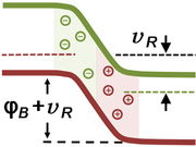
In reverse bias the occupancy level for holes again tends to stay at the level of the bulk p-type semiconductor while the occupancy level for electrons follows that for the bulk n--type. In this case, the p-type bulk band edges are raised relative to the n-type bulk by the reverse bias vR, so the two bulk occupancy levels are separated again by an energy determined by the applied voltage. As shown in the diagram, this behavior means the step in band edges is increased to φB+vR, and the depletion region widens as holes are pulled away from it on the p-side and electrons on the n-side.
When the reverse bias is applied, the electric field in the depletion region is increased, pulling the electrons and holes further apart than in the zero bias case. Thus, any current that flows is due to the very weak process of carrier generation inside the depletion region due to generation-recombination defects in this region. That very small current is the source of the leakage current under reverse bias. In the photodiode, reverse current is introduced using creation of holes and electrons in the depletion region by incident light, thus converting a portion of the incident light into an electric current.
When the reverse bias becomes very large, reaching the breakdown voltage, the generation process in the depletion region accelerates leading to an avalanche condition which can cause runaway and destroy the diode.
Diode law
The DC current-voltage behavior of the ideal pn-diode is governed by the Shockley diode equation:[3]
with vD the DC voltage across the diode, and IR the reverse saturation current, the current that flows when the diode is reverse biased (vD large and negative). The symbol Vth denotes the thermal voltage, Vth=kBT/q ≈ 25 mV at T=290 kelvins.
This equation does not model the non-deal behavior such as excess reverse leakage or breakdown phenomena. In many practical diodes this equation must be modified to read:
where the ideality factor, n is introduced to model a slower rate of increase than predicted by the ideal diode law. Using this equation, the diode on-resistance is:
exhibiting a lower resistance the higher the current.
Capacitance
The depletion layer between the n- and p-sides of a pn-junction serves as an insulating region that separates the two diode contacts. Thus, the diode in reverse bias exhibits a depletion-layer capacitance, analogous to a parallel plate capacitor with a dielectric spacer between the contacts. In reverse bias the width of the depletion layer is widened with increasing reverse bias, and the capacitance is accordingly decreased. Thus, the junction serves as a voltage-controllable capacitor.
In forward bias, besides the above depletion-layer capacitance, minority carrier charge injection and diffusion occurs. A diffusion capacitance exists expressing the change in minority carrier charge that occurs with a change in forward bias. In terms of the stored minority carrier charge, the diode current iD is:
where QD is the charge associated with diffusion of minority carriers, and τT is the transit time, the time taken for the minority charge to transit the injection region. Typical values for transit time are 0.1–100 ns.[4] On this basis, the diffusion capacitance is calculated to be:
Generally speaking, for usual current levels in forward bias, this capacitance far exceeds the depletion-layer capacitance.
Transient response
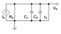
Small-signal circuit for pn-diode driven by a current signal represented as a Norton source.
The diode is a highly non-linear device, but for small-signal variations its response can be analyzed using a small-signal circuit based upon the DC bias about which the signal is imagined to vary. The equivalent circuit is shown at the right for a diode driven by a Norton source. Using Kirchhoff's current law at the output node:
with CD the diode diffusion capacitance, CJ the diode junction capacitance (the depletion layer capacitance) and rD the diode resistance, all at the selected quiescent bias point or Q-point. The output voltage provided by this circuit is then:
with (RS||rD) the parallel combination of RS and rD. This transresistance amplifier exhibits a corner frequency fC:
and for frequencies f >> fC the gain rolls off with frequency as the capacitors short-circuit the resistor rD. Assuming, as is the case when the diode is turned on, that CD>>CJ and RS>>rD, the expressions found above for the diode resistance and capacitance provide:
which relates the corner frequency to the diode transit time τT.
Notes
- ↑ Jump up to: 1.0 1.1 John Sparkes (1994). Semiconductor Devices, 2nd ed. CRC Press, p. 78. ISBN 0748773827.
- ↑ Naturally, this voltage depends upon the selected current level. This voltage for the pn-junction diode is taken variously as 0.7 V and 0.5 V; see AS Sedra and KF Smith (1998). “Chapter 3: Diodes”, Microelectronic circuits, 4th ed. Oxford University Press, p. 134 & Figure 3.8. ISBN 0195116631. .
- ↑ Andrei Grebennikov (2011). “§2.1.1: Diodes: Operational principle”, RF and Microwave Transmitter Design. J Wiley & Sons, p. 59. ISBN 047052099X.
- ↑ Narain Arora (2007). Mosfet modeling for VLSI simulation: theory and practice. World Scientific, p. 539. ISBN 981256862X. Jean-Pierre Colinge, Cynthia A. Colinge (2002). Physics of semiconductor devices, 2nd ed. Springer, p. 149. ISBN 1402070187.

