Schottky diode: Difference between revisions
imported>John R. Brews (→Barrier height: paragraphing) |
imported>John R. Brews (→Zero bias: re-arrange sentences) |
||
| Line 35: | Line 35: | ||
====Zero bias==== | ====Zero bias==== | ||
The figure | The formation of a Schottky barrier is shown schematically in the figure, beginning with the isolated materials (top), an intermediate dipole formation stage (center), and the completed configuration with formation of a depletion layer (bottom). The dipole layer still is present in the bottom figure, but is omitted for clarity. The figure is not intended to indicate exactly how the processes occur with increasing proximity of the materials, but merely the processes involved. | ||
Ordinarily, the Fermi levels of different materials differ. When they are brought into electrical contact, enabling electron transfer between the materials, the work done in removing an electron from one material and placing it in the other is equal to the energy difference in the Fermi levels. Consequently, energy is released upon contact by electron transference from the material with the higher Fermi level to the material with the lower Fermi level. This charge transfer continues until the electrical charge difference means the energy gain from transfer is countered by the electrical work required against the charge difference. At this point the two Fermi levels are brought into coincidence at a common level ''E<sub>F</sub>'' | Ordinarily, the Fermi levels of different materials differ. When they are brought into electrical contact, enabling electron transfer between the materials, the work done in removing an electron from one material and placing it in the other is equal to the energy difference in the Fermi levels. Consequently, energy is released upon contact by electron transference from the material with the higher Fermi level to the material with the lower Fermi level. This charge transfer continues until the electrical charge difference means the energy gain from transfer is countered by the electrical work required against the charge difference. At this point the two Fermi levels are brought into coincidence at a common level ''E<sub>F</sub>'' and no further charge transfer occurs. This flat Fermi level situation corresponds to [[thermal equilibrium]], and no net current flows once equilibrium is reached. | ||
The figure shows (top) a charge-neutral, partly filled metal energy band and a charge-neutral semiconductor valence and conduction band, electrically isolated from each other. The Fermi level in the ''p''-type semiconductor ''E<sub>Fp</sub>'' (assumed to be in units of eV) is near its valence band edge, as set by its acceptor impurity doping. (See [[Fermi function#Fermi level|Fermi level]]). The Fermi level in the metal ''E<sub>Fm</sub>'' marks the top of the filled electron energy levels in a partly filled band of the metal. | |||
The | The properties of the bulk materials do not determine by themselves the charge transfer between them that occurs upon forming electrical contact. In fact, the chemistry of the interface, defects at the interface, and the mechanical adaptation to new atomic positions near the interface that are differently spaced than those found in bulk material, all conspire to alter the amount of charge transfer from that expected from bulk properties, and these effects are approximately represented as a charged dipole layer, as shown in the center panel.<ref name=interface> | ||
The | For further discussion, see for example, {{cite book |title=Silicon Materials Science and Technology X, Issue 2 |chapter=Electrical properties: Partial charge transfer in interface bonds |url=http://books.google.com/books?id=KqIa5SCP93sC&pg=PA195#v=onepage&q&f=false |pages=p. 195 |author=Howard R. Huff, H. Iwai, H. Richter |isbn=156677439X |publisher=The Electrochemical Society |year=2006}}{{cite journal |title=Recent advances in Schottky barrier concepts |author=Raymond T Tung |journal=Materials Science and Engineering: R: Reports |doi=10.1016/S0927-796X(01)00037-7 |url=http://www.sciencedirect.com/science?_ob=ArticleURL&_udi=B6TXH-43VKKX9-1&_user=9555371&_coverDate=11%2F09%2F2001&_rdoc=1&_fmt=high&_orig=search&_origin=search&_sort=d&_docanchor=&view=c&_acct=C000055186&_version=1&_urlVersion=0&_userid=9555371&md5=65ce8645617ec3e07be3857043c4278a&searchtype=a|volume=vol. 35 |issue=1-3 |pages=pp. 1-138 |year=2001 |publisher=Elsevier Science}}{{cite journal |title=Molecules and electronic materials |author=David Cahen, Gary Hodes |url=http://onlinelibrary.wiley.com/doi/10.1002/1521-4095%2820020605%2914:11%3C789::AID-ADMA789%3E3.0.CO;2-H/abstract |journal=Advanced materials progress report |pages=pp. 789-798 |date=2002-06-05 |volume=vol. 14 |issue=No. 11 |publisher=Wiley-VCH}} [http://dx.doi.org/ DOI:] 10.1002/1521-4095(20020605)14:11<789::AID-ADMA789>3.0.CO;2-H | ||
</ref> As the materials mate, this interfacial dipole layer adjusts the Fermi level separation, determining the necessary remaining charge transfer that forms the depletion layer. This interface dipole contribution is specific to the interface materials, and is different for (say) a material interface cleaved in vacuum and that for the same material mated to some other material. This interface dipole also is different for differently oriented crystal planes. But whatever the amount of charge transfer, charge transfer occurs and the two adjoined materials each acquire a charge. | |||
The bottom panel shows the final configuration. The transfer of electrons from the metal results in a very thin layer of positive charge in the metal very near the interface. Because the electron density in the metal is extremely large, the band bending in the metal is negligible in the diagram. On the other hand, the density of holes in the semiconductor is not nearly as large as the electron density in the metal, so the charging of the semiconductor is spread deeply into the material (the [[field effect]]). The semiconductor gains electrons, as indicated by the bending of the valence band edge away from the Fermi level, which increases the valence band occupancy by electrons. Differently stated, the vacancies (holes) in the valence band are reduced in number, and the charge balance in the band-bending region is lost. In this ''depletion layer'', the holes or ''majority carriers'' are depleted (the unshaded surface region in the figure), exposing the immobile negative acceptor dopant ions to make this region charge-negative. This dopant charge results in a potential according to [[Maxwell equations#Poisson's equation|Poisson's equation]]. The potential decreases with distance toward the bulk semiconductor, and at some distance (the ''depletion width'') the bulk properties of the semiconductor are regained and the semiconductor bulk is charge neutral. | |||
</ | The final potential barrier height between the metal Fermi level and the majority carrier band edge in the semiconductor is called the ''Schottky barrier height'', labeled ''φ<sub>B</sub>'' in the figure. It is a form of [[contact potential]]. The concomitant potential drop across the semiconductor depletion layer is called the ''built-in'' potential, labeled ''φ<sub>bi</sub>'' in the figure. | ||
At zero bias there is no net current, because the current from the semiconductor is balanced by that from the metal. According to the model of [[thermionic emission]], the current flowing over an energy barrier is proportional to the carrier density next to the barrier. One can imagine the carriers in rapid thermal motion randomly directed. The carriers approaching the barrier with energies lower than the barrier height bounce off the barrier and do not cross it. Some fraction of those that are more energetic escape backward scattering to succeed in surmounting the barrier, and are lost to the far side. On the metal side, hole injection from the metal Fermi level into the semiconductor valence band is small as it requires surmounting a large energy barrier. On the semiconductor side, hole injection into the metal requires surmounting the built-in barrier height, ''φ<sub>bi</sub>''. Although the barrier on the semiconductor side is smaller than the Schottky barrier ''φ<sub>B</sub>'' on the metal side, so is the carrier density. The two currents balance at zero bias, so no net current flows. These balancing current flows are much larger than in the [[semiconductor diode|''pn''-diode]] because thermionic emission results in larger currents than the diffusion-recombination mechanism of the ''pn''-diode.<ref name=saturation> | At zero bias there is no net current, because the current from the semiconductor is balanced by that from the metal. According to the model of [[thermionic emission]], the current flowing over an energy barrier is proportional to the carrier density next to the barrier. One can imagine the carriers in rapid thermal motion randomly directed. The carriers approaching the barrier with energies lower than the barrier height bounce off the barrier and do not cross it. Some fraction of those that are more energetic escape backward scattering to succeed in surmounting the barrier, and are lost to the far side. On the metal side, hole injection from the metal Fermi level into the semiconductor valence band is small as it requires surmounting a large energy barrier. On the semiconductor side, hole injection into the metal requires surmounting the built-in barrier height, ''φ<sub>bi</sub>''. Although the barrier on the semiconductor side is smaller than the Schottky barrier ''φ<sub>B</sub>'' on the metal side, so is the carrier density. The two currents balance at zero bias, so no net current flows. These balancing current flows are much larger than in the [[semiconductor diode|''pn''-diode]] because thermionic emission results in larger currents than the diffusion-recombination mechanism of the ''pn''-diode.<ref name=saturation> | ||
Revision as of 09:37, 7 February 2011
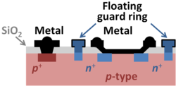
The Schottky diode is a two-terminal device consisting of conductive gate (for example, a metal) on top of a semiconductor body. It is named after Walter H Schottky, who proposed a detailed theory for point contact rectification in 1938.[1] The modern theory of Schottky diode operation was contributed by Hans Bethe in 1942.[2] A generic name for this structure is the metal-semiconductor diode or M/S diode.[3] For low voltage applications, below 200V, silicon is used, but for higher voltages (up to 3000 V or more) silicon carbide is used to extend the breakdown voltage. These voltages are achievable only when edge breakdown is avoided, which requires special attention to edge termination designs.[4] The figure shows three strategies toward increasing the edge breakdown voltage: an extension of the metal diode contact over a tapered oxide and also an n+-guard ring and a floating guard ring. These strategies are sometimes used together, but also are used separately. The substrate contact is made through an ohmic contact to the p-substrate made using a metal-to-p+ region on the surface of the diode, that is, a contact with a linear current-voltage characteristic like that of a resistor.
Although the example used in this article is a Schottky diode on a p-type substrate, Schottky diodes on n-type substrates are more common.
Applications
The Schottky diode is used in a large variety of applications, ranging from practical devices for switching, rectification and photo-detection, to test structures for fabrication monitoring and for studies of semiconductor defects and processes.
Operation
Three different bias cases are examined: zero bias, forward bias, and reverse bias. A simplified one dimensional analysis along a line vertically through the center of the Schottky contact is used throughout. It is imagined that the p+-ohmic contact is vertically below the Schottky contact.
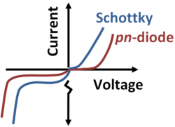
As seen in the comparison with the pn-diode shown in the figure, the Schottky diode tends to turn on at lower forward voltages but rises more slowly because of the nonideality factor noted later. The Schottky diode also tends to have a higher reverse leakage current. The mechanism for current flow is different in the two devices: the pn-diode current is diffusion driven by carrier concentration differences, while the Schottky diode is driven by thermionic emission, that is, the surmounting of a potential barrier by energetic carriers. This mechanism is described further below.
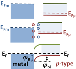
Schottky barrier formation on p-type semiconductor. Top: isolated charge-neutral bulk materials. Center: dipole layer formed as materials interact; Fermi level difference is reduced. Bottom: final configuration following charge transfer to reach equilibrium with no applied voltage. The neutral (shaded) region in the semiconductor moves away from the interface, leaving a charged depletion region (unshaded) near the interface. Energies are in eV.
Zero bias
The formation of a Schottky barrier is shown schematically in the figure, beginning with the isolated materials (top), an intermediate dipole formation stage (center), and the completed configuration with formation of a depletion layer (bottom). The dipole layer still is present in the bottom figure, but is omitted for clarity. The figure is not intended to indicate exactly how the processes occur with increasing proximity of the materials, but merely the processes involved.
Ordinarily, the Fermi levels of different materials differ. When they are brought into electrical contact, enabling electron transfer between the materials, the work done in removing an electron from one material and placing it in the other is equal to the energy difference in the Fermi levels. Consequently, energy is released upon contact by electron transference from the material with the higher Fermi level to the material with the lower Fermi level. This charge transfer continues until the electrical charge difference means the energy gain from transfer is countered by the electrical work required against the charge difference. At this point the two Fermi levels are brought into coincidence at a common level EF and no further charge transfer occurs. This flat Fermi level situation corresponds to thermal equilibrium, and no net current flows once equilibrium is reached.
The figure shows (top) a charge-neutral, partly filled metal energy band and a charge-neutral semiconductor valence and conduction band, electrically isolated from each other. The Fermi level in the p-type semiconductor EFp (assumed to be in units of eV) is near its valence band edge, as set by its acceptor impurity doping. (See Fermi level). The Fermi level in the metal EFm marks the top of the filled electron energy levels in a partly filled band of the metal.
The properties of the bulk materials do not determine by themselves the charge transfer between them that occurs upon forming electrical contact. In fact, the chemistry of the interface, defects at the interface, and the mechanical adaptation to new atomic positions near the interface that are differently spaced than those found in bulk material, all conspire to alter the amount of charge transfer from that expected from bulk properties, and these effects are approximately represented as a charged dipole layer, as shown in the center panel.[5] As the materials mate, this interfacial dipole layer adjusts the Fermi level separation, determining the necessary remaining charge transfer that forms the depletion layer. This interface dipole contribution is specific to the interface materials, and is different for (say) a material interface cleaved in vacuum and that for the same material mated to some other material. This interface dipole also is different for differently oriented crystal planes. But whatever the amount of charge transfer, charge transfer occurs and the two adjoined materials each acquire a charge.
The bottom panel shows the final configuration. The transfer of electrons from the metal results in a very thin layer of positive charge in the metal very near the interface. Because the electron density in the metal is extremely large, the band bending in the metal is negligible in the diagram. On the other hand, the density of holes in the semiconductor is not nearly as large as the electron density in the metal, so the charging of the semiconductor is spread deeply into the material (the field effect). The semiconductor gains electrons, as indicated by the bending of the valence band edge away from the Fermi level, which increases the valence band occupancy by electrons. Differently stated, the vacancies (holes) in the valence band are reduced in number, and the charge balance in the band-bending region is lost. In this depletion layer, the holes or majority carriers are depleted (the unshaded surface region in the figure), exposing the immobile negative acceptor dopant ions to make this region charge-negative. This dopant charge results in a potential according to Poisson's equation. The potential decreases with distance toward the bulk semiconductor, and at some distance (the depletion width) the bulk properties of the semiconductor are regained and the semiconductor bulk is charge neutral.
The final potential barrier height between the metal Fermi level and the majority carrier band edge in the semiconductor is called the Schottky barrier height, labeled φB in the figure. It is a form of contact potential. The concomitant potential drop across the semiconductor depletion layer is called the built-in potential, labeled φbi in the figure.
At zero bias there is no net current, because the current from the semiconductor is balanced by that from the metal. According to the model of thermionic emission, the current flowing over an energy barrier is proportional to the carrier density next to the barrier. One can imagine the carriers in rapid thermal motion randomly directed. The carriers approaching the barrier with energies lower than the barrier height bounce off the barrier and do not cross it. Some fraction of those that are more energetic escape backward scattering to succeed in surmounting the barrier, and are lost to the far side. On the metal side, hole injection from the metal Fermi level into the semiconductor valence band is small as it requires surmounting a large energy barrier. On the semiconductor side, hole injection into the metal requires surmounting the built-in barrier height, φbi. Although the barrier on the semiconductor side is smaller than the Schottky barrier φB on the metal side, so is the carrier density. The two currents balance at zero bias, so no net current flows. These balancing current flows are much larger than in the pn-diode because thermionic emission results in larger currents than the diffusion-recombination mechanism of the pn-diode.[6]
Evidently the charge transfer between the metal and the semiconductor determines the Schottky barrier height φB. While this barrier height is very influential in determining the current, other interfacial properties also help to decide just how much current will be injected at a given barrier height, sometimes lumped into a factor called the "generalized Richardson constant", named after the Nobel Prize winning author of the original theory of thermionic emission, Owen Willans Richardson. However, in real devices thermionic emission is complicated by the effects of diffusion, barrier shape, field emission, homogeneity of the interface, and so forth.[7] Calculation of the barrier height based upon a fundamental understanding either of current balance or of charge transfer should lead to the same result, but at present such detailed calculations remain topics for research.
Forward bias
Under forward bias, a net current of holes now flows from the semiconductor to the metal (or, equivalently, of electrons from the metal to the semiconductor), as explained next.
If a forward bias voltage is applied VF, the Fermi level of the bulk metal EFm (in eV) is raised in energy above the bulk Fermi level in the semiconductor EFp, which lowers the potential drop across the depletion layer to a value φbi−VF. Notice that the alignment of the metal Fermi level relative to the semiconductor band edges at the interface is not changed by the bias: that is, φB is fixed by the processes involved in adjusting the Fermi levels to achieve equilibrium at zero applied bias. That fixed alignment means the barrier for hole injection from the metal into the semiconductor is not changed by an applied bias, and the injected hole current from the metal remains the same as at zero bias.
At zero bias there is no net current, because the current from the semiconductor is balanced by that from the metal. But under forward bias the current from the metal side is unaffected (and extremely small), while that on the semiconductor side is increased by the forward bias. According to the model of thermionic emission, the electrical current injected from the semiconductor is proportional to the hole density at the interface. Using a simple Boltzmann approximation to the Fermi function, the hole density on the semiconductor side is increased by a factor:
where p(0) is the zero forward bias value of hole density on the semiconductor side. The hole current from the semiconductor to the metal therefore is increased by this factor. The current, being by convention a flow of positive charge, is therefore positive from the semiconductor to the metal, and the Schottky barrier current in forward bias becomes:
where I(0) is related to the zero-bias current exchange between the two materials.
Due to some complications of real Schottky barriers, the current is usually represented as:
where the factor n is usually larger than one and is called the ideality factor.
Reverse bias
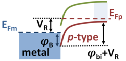
If a reverse bias VR is applied, the Fermi level of the metal is lowered below that of the semiconductor, and the barrier height for holes is increased on the semiconductor side by the amount of the reverse bias. The hole density is therefore decreased compared to equilibrium (the electron occupancy increases) and the current from the semiconductor falls below the equilibrium value. That means the diode current changes direction compared to the forward biased case.
If the diode were ideal, the current in reverse bias would be simply −I(0), the hole current backward injected by the metal into the semiconductor at zero bias, because the the hole current from the semiconductor side is completely suppressed by the very low hole density at the interface in reverse bias, making the injection of holes into the metal nearly zero. However, in practice, in reverse bias a leakage current is drawn due to generation of electrons and holes by defects in the depletion layer. If a large enough reverse voltage is applied, breakdown occurs, due to runaway of the generation mechanisms, or more commonly, due to edge breakdown in the high field region near the contact perimeter. A brief outline of the breakdown phenomena follows.[8]
Under reverse bias, a large electric field is present in the depletion layer, and carriers in the depletion layer are accelerated by this field. The carriers gain energy from the field, but they lose energy by creating vibrations in the semiconductor lattice, called phonons, thereby heating up the material. However, as the field increases with application of a larger reverse bias voltage, an increased fraction of the high energy carriers fail to lose energy by phonon creation, attaining energies in excess of the material bandgap. These energetic carriers, instead of losing energy to phonons, lose energy by creating electron-hole pairs, a process called impact ionization. At a crucial breakdown field, these generated carrier pairs themselves generate pairs and the process enters runaway.
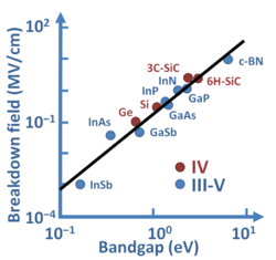
A wider bandgap material like SiC has a higher intrinsic breakdown voltage than a lower bandgap material like Si because the energy to make an electron-hole pair scales with the bandgap. An electron created by impact ionization is in the conduction band, and the associated hole is in the valence band, and these two are separated in energy by at least the bandgap energy. This bandgap energy is provided by the electric field inside the depletion layer, which must accelerate the impacting carrier beyond this energy before generation can occur. The figure shows a log-log plot of field upon the bandgap energy fitted to an empirical power law with exponent 2.4.[9]
Unlike the MOSFET or the MOS capacitor, the expansion of the depletion layer width in response to an applied reverse bias is not arrested at large biases by formation of an inversion layer, a thin surface layer at the interface made up of minority carriers (electrons in a p-type semiconductor). An inversion layer cannot form, because the carriers are transmitted to the metal, and cannot be stored at the interface.
Transient response
A Schottky diode in forward bias conducts a current. This current can be cut off by switching to a reverse bias. The response time of the diode is simply the time it takes for the holes to move back from the edge of the narrow depletion region of forward bias to the edge of the wider depletion region of reverse bias. This switching is very rapid, the switching time given by the RC time constant of the diode, where R is the resistance of the bulk p-type material, and C is the diode capacitance. To understand the nature of this capacitance, note that the majority carriers in the semiconductor (holes in this example) are separated from the metal contact by the insulating depletion layer, where there are only immobile dopant ions, and no mobile carriers. Thus, the diode represents an electrical capacitor with two plates, namely the metal and the neutral bulk material, separated by a dielectric, namely the insulating depletion region.
Compared to the MOS capacitor, or the pn-diode or the bipolar transistor, this switching time is very fast because it is not limited by the response time of minority carriers, which have to be removed from those devices by slow recombination processes.
Barrier height
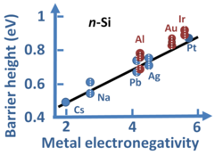
From the very earliest work of Schottky, Mott and Davydov it was expected that the Schottky barrier height would depend upon the electronegativity of the metal contact, as that measures the tendency of the metal to grab electrons. The figure shows that a correlation is observed, but the dependence is not as strong as originally thought because of the influence of the details of the interface charge distribution.[10] The slope of this line is about 0.1, while the original Schottky-Mott rule proposed a slope of 1. In the figure, multiple barrier heights for the same metal are observed, corresponding to different interface structures.
The theory behind the straight line in the figure is based upon dividing electronic states at the metal semiconductor interface into four groups: (i) electron states in the metal, called the metal-induced gap states (MIGS), which have an amplitude that decays into the semiconductor (ii) electron states in the semiconductor that decay into the metal, (iii) localized states that decay from the interface both into the metal and into the semiconductor, and finally (iv) those states that are bulk-like in both materials and decay in neither one. The theory plotted in the figure, the MIGS theory, suggests that the barrier height is determined primarily by the first group of states.[10]
A simplified version of this model predicts an interface charge dipole that results from the negative charge in the MIGS and the positive image charge reflected in the metal itself. This interface dipole reduces the initial mismatch between the semiconductor and the metal Fermi levels, reducing the amount of charge transfer that creates the depletion layer. An overview and assessment of this theory is provided by Tung, who emphasizes that the MIGS are an interface property and depend upon both the metal and the semiconductor.[11]
Notes
- ↑ W. Schottky (1939). "Zur Halbleitertheorie der Sperrschicht- und Spitzengleichrichter". Zeitschrift für Physik A Hadrons and Nuclei vol. 113: pp. 813 ff. DOI:10.1007/BF01340116. Research Blogging. W. Schottky (1941). "Vereinfachte und erweiterte Theorie der Randschicht-gleichrichter". Zeitschrift für Physik A Hadrons and Nuclei vol. 118: pp. 539 ff. DOI:10.1007/BF01329843. Research Blogging. See also E. Spenke (1949). "Zur Randschichttheorie der Trockengleichrichter". Z. Physik vol. 126: pp. 67 ff. DOI:10.1007/BF01331042. Research Blogging.
- ↑ HA Bethe (November, 1942). "MIT Radiation Lab. Report" vol. 43-12.
- ↑ The term "Schottky diode" may be taken erroneously to refer to diffusion as the mechanism of operation as first proposed by Mott, Schottky and Davydov. However, the mechanism in most devices is a combination of thermionic emission and diffusion, as later proposed by Bethe, the so-called thermionic-diffusion theory. See Chih-Tang Sah (1991). “§560: Metal/semiconductor diode”, Fundamentals of solid-state electronics. World Scientific, p. 474. ISBN 9810206372. and SM Sze and KK Ng (2007). “Chapter 3 Metal-semiconductor contacts”, Physics of semiconductor devices, 3rd ed. Wiley, pp. 134 ff. ISBN 0471143235.
- ↑ B. Jayant Baliga (2005). “§3.2 Schottky diode edge terminations”, Silicon carbide power devices. World Scientific, pp. 44 ff. ISBN 9812566058.
- ↑ For further discussion, see for example, Howard R. Huff, H. Iwai, H. Richter (2006). “Electrical properties: Partial charge transfer in interface bonds”, Silicon Materials Science and Technology X, Issue 2. The Electrochemical Society, p. 195. ISBN 156677439X. Raymond T Tung (2001). "Recent advances in Schottky barrier concepts". Materials Science and Engineering: R: Reports vol. 35 (1-3): pp. 1-138. DOI:10.1016/S0927-796X(01)00037-7. Research Blogging. David Cahen, Gary Hodes (2002-06-05). "Molecules and electronic materials". Advanced materials progress report vol. 14 (No. 11): pp. 789-798. DOI: 10.1002/1521-4095(20020605)14:11<789::AID-ADMA789>3.0.CO;2-H
- ↑ See the discussion in the general reference by CT Sah, p. 489.
- ↑ Raymond T Tung (November 2001). "Recent advances in Schottky barrier concepts". Materials Science and Engineering: R: Reports vol. 35 (Nos. 1-3): pp. 1-138. DOI:10.1016/S0927-796X(01)00037-7. Research Blogging.
- ↑ A discussion is found, for example, in Yuan Taur, Tak H Ning (2005). “§2.4 High-field effects”, Fundamentals of modern VLSI devices. Cambridge University Press, pp. 90 ff. ISBN 9780521559591.
- ↑ Sadao Adachi (2005). “Figure 9.11”, Properties of group-IV, III-V and II-VI semiconductors. Wiley. ISBN 0470090324.
- ↑ 10.0 10.1 Winfried Mönch (2001). “Figure 19.18”, Semiconductor Surfaces and Interfaces, 3rd ed. Springer, p. 412. ISBN 3540679022.
- ↑ Raymond T Tung (2001). "Previously cited paper; §4: Models on bonds and dipoles at MS interfaces". Materials Science and Engineering: R: Reports vol. 35 (1-3): pp. 1-138. DOI:10.1016/S0927-796X(01)00037-7. Research Blogging.
